科技工作者之家
科技工作者之家APP是专注科技人才,知识分享与人才交流的服务平台。
科技工作者之家 2019-06-10
来源:中科院半导体所
半导体薄膜异质外延的最新进展在最新出版的《半导体学报》2019年第6期上,中国科学院上海技术物理研究所顾溢研究员介绍了半导体薄膜异质外延的最新进展。高质量半导体薄膜异质外延是制备半导体器件的基础。针对晶格失配衬底上的半导体薄膜异质外延,研究人员发展了多种预处理方法和异变缓冲层结构来提高外延质量,并已实现了多种光电器件和电子器件。最新发展的基于二维材料中间层的异质外延是值得关注的一个方向,如果取得突破,将实现在任意衬底上外延高质量半导体薄膜。
最近,基于石墨烯等二维材料中间层外延高质量GaN薄膜和发光二极管材料已经取得了很大进展。然而,在二维材料中间层上外延GaAs等其他半导体材料由于原子吸附能和迁移能的限制仍面临挑战,需要从理论和实验上进一步研究成核层、二维材料参数和二维/三维界面等关键问题。
The heteroepitaxy of semiconductor thin films is a cornerstone of semiconductor devices and is naturally preferred to grow on matched substrates from the view point of material epitaxy. However, the heteroepitaxy is always performed on mismatched substrates due to the limited choices of mature substrates, which constrains the quality of semiconductor thin films. In past decades, numerous metamorphic buffer layers and pre-growth processing have been developed to control the defect density in the epitaxial semiconductor thin films on heterogeneous mismatched substrates. Through these approaches, some kinds of semiconductor lasers, detectors and electronic devices with high performances have been achieved and applied in industry. However, people are always keeping a dream to epitaxially grow high quality semiconductor thin films on arbitrary substrates. The heteroepitaxy through two-dimensional (2D) materials could be a potential route. If one can grow sp3-bonded three-dimensional (3D) epitaxial films on 2D materials, the limitation of matched substrates will be overcome. Furthermore, the transfer of single-crystalline semiconductor thin films will be allowed due to the weak van der Waals interaction.
High quality GaN thin films with low threading dislocations and light emitting diodes (LEDs) with high performances and flexibility have been demonstrated on many substrates through graphene and other 2D materials, causing the researches on this topic grow rapidly. The interfacial buffers or artificial treatments are usually employed for the heteroepitaxy to achieve periodic nucleation sites between the 3D and 2D materials. Then there comes a question whether other semiconductor thin films, e.g. another widely used III–V semiconductor GaAs, are able to grown on mismatched substrates through 2D materials. The answer is: possible but difficult.
Although a number of studies have been undertaken to achieve high quality GaAs nanowire on graphene, the single-crystalline thin films are attractive to demonstrate high performance devices. In 2014, Alaskar et al. reported GaAs single-crystalline thin films with smooth morphology on Si substrate through multilayer graphene as shown in Fig. 1. From their theoretical calculation, the 2D growth of III–arsenide films encounters much larger challenges than III–nitrides due to the much lower adsorption and migration energy as well as lower ratio of adsorption energy to bulk cohesive energy for III–arsenides. The smooth GaAs single-crystalline thin films were grown on multiplayer graphene/Si by using Ga-prelayer and delicately controlled growth temperature. In 2017, Kim et al. reported that GaAs homoepitaxial single-crystalline films was able to achieve on GaAs substrates through monolayer graphene, and an epitaxial alignment of Ga atoms to As atoms was found, which is also applicable to the cases of InP and GaP. The so-called “remote epitaxy” technique enables the copy of semiconductor films from underlying substrates and is attractive in the re-using of graphene-coated substrates. More recently, the effects of polarity on the remote epitaxy of semiconductor thin films on 2D material coated substrates are investigated, and the types of single-crystalline thin films suitable for this technique are predicted by Kong et al. The potential field from ionic-bonded materials was found strong enough topenetrate through a few layers of graphene. They claimed that for the lattice mismatched system of GaN-GaAs, the nuclei-substrate interaction did not increase with the size of nuclei, and the enhancement of potential energy fluctuation was prevented by the mismatch-induced broad distribution of local dipole alignments.
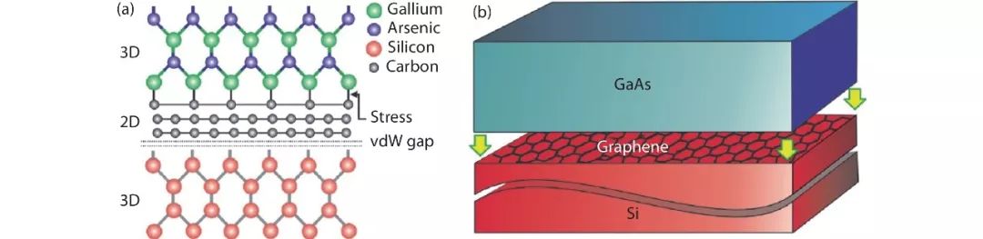
Figure1. (Color online) (a) Schematic atomic geometry and (b) schematic epitaxial structure of GaAs thin film on graphene-coated Si substrate[3].
In the case of semiconductor thin films epitaxially grown on mismatched substrates, the use of metamorphic buffer is still, and will be for a long time, the main route for mass production. However, the heteroepitaxy through 2D material buffer is very attractive. Recent advances have confirmed the possibility of this promising route, while following main questions need to be further addressed:
1) The applicable nucleation sites for the heteroepitaxy of different semiconductor thin films. Defects of 2D materials, nanowire structures, potential field of substrates, or others?
2) The effects of different 2D materials and substrates, including the layer number of 2D materials, the acquisition and pre-growth treatment methods of 2D materials, etc.
3) The interaction of epitaxial 3D thin films with local 2D materials. The alloy atoms as well as dislocations, stacking faults and other crystal defects all need to be considered.
References:
[1] Chung K, Lee C H, Yi G C. Transferable GaN layers grown on ZnO-coated graphene layers for optoelectronic devices. Science, 2010, 330, 655
[2] Kim J, Bayram C, Park H, et al. Principle of direct van der Waals epitaxy of single-crystalline films on epitaxial graphene. Nat Commun, 2014, 5, 4836
[3] Alaskar Y, Arafin S, Wickramaratne D, et al. Towards van der Waals epitaxial growth of GaAs on Si using a graphene buffer layer. Adv Funct Mater, 2014, 24, 6629
[4] Kim Y, Cruz S, Lee K, et al. Remote epitaxy through graphene enables two-dimensional material-based layer transfer. Nature, 2017, 544, 340
[5] Kong W, Li H, Qiao K, et al. Polarity governs atomic interaction through two-dimensional materials. Nat Mater, 2018, 17, 999
点击阅读顾溢研究员文章:
Heteroepitaxy of semiconductor thin films
Yi Gu
J. Semicond. 2019, 40(6), 060401
doi: 10.1088/1674-4926/40/6/060401
来源:bdtdsj 中科院半导体所
原文链接:http://mp.weixin.qq.com/s?__biz=MzI1OTExNzkzNw==&mid=2650448881&idx=2&sn=8499a28f921b077f4b2e9e330014a008&chksm=f273c5efc5044cf93e7b1ef70eea57755fc7bb08fe8ee376aacafe5ded8caec9219dfd23614d&scene=27#wechat_redirect
版权声明:除非特别注明,本站所载内容来源于互联网、微信公众号等公开渠道,不代表本站观点,仅供参考、交流、公益传播之目的。转载的稿件版权归原作者或机构所有,如有侵权,请联系删除。
电话:(010)86409582
邮箱:kejie@scimall.org.cn


科技工作者之家APP是专注科技人才,知识分享与人才交流的服务平台。
 微信
微信
 京公网安备11010202008424号