科技工作者之家
科界APP是专注科技人才,知识分享与人才交流的服务平台。
科技工作者之家 2020-04-05
来源:知社学术圈
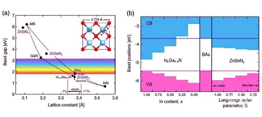
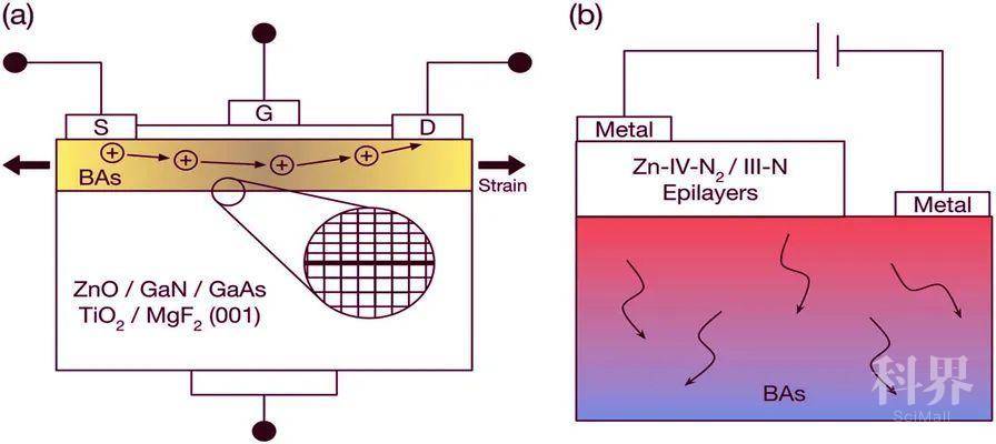
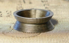
砷化硼是近期受到广泛关注一种III-V半导体材料。研究表明,砷化硼具有可媲美金刚石的超高热导率(~1300 Wm-1K-1),同时具有本征p型导电特性,并且可以长成毫米级的单晶。目前人们对砷化硼的基本物理性质已经开展了较为广泛的研究。然而,从光电器件应用考虑,不论作为功能薄膜还是衬底,砷化硼都必须与其他半导体材料形成异质结,因此考察其异质结相关特性十分重要。
Boron arsenide heterostructures: lattice-matched heterointerfaces and strain effects on band alignments and mobility
Kyle Bushick, Sieun Chae, Zihao Deng, John T. Heron& Emmanouil Kioupakis
BAs is a III–V semiconductor with ultra-high thermal conductivity, but many of its electronic properties are unknown. This work applies predictive atomistic calculations to investigate the properties of BAs heterostructures, such as strain effects on band alignments and carrier mobility, considering BAs as both a thin film and a substrate for lattice-matched materials. The results show that isotropic biaxial in-plane strain decreases the band gap independent of sign or direction. In addition, 1% biaxial tensile strain increases the in-plane electron and hole mobilities at 300 K by >60% compared to the unstrained values due to a reduction of the electron effective mass and of hole interband scattering. Moreover, BAs is shown to be nearly lattice-matched with InGaN and ZnSnN2, two important optoelectronic semiconductors with tunable band gaps by alloying and cation disorder, respectively. The results predict type-II band alignments and determine the absolute band offsets of these two materials with BAs. The combination of the ultra-high thermal conductivity and intrinsic p-type character of BAs, with its high electron and hole mobilities that can be further increased by tensile strain, as well as the lattice-match and the type-II band alignment with intrinsically n-type InGaN and ZnSnN2 demonstrate the potential of BAs heterostructures for electronic and optoelectronic devices.
来源:zhishexueshuquan 知社学术圈
原文链接:https://mp.weixin.qq.com/s?__biz=MzIwMjk1OTc2MA==&mid=2247502218&idx=3&sn=ba360e401f4f5262f5306387040d1a3f&chksm=96d43775a1a3be63a69a153ca7af3f93cf95d4a670981a07f256d34f1830c910453459c93ec4#rd
版权声明:除非特别注明,本站所载内容来源于互联网、微信公众号等公开渠道,不代表本站观点,仅供参考、交流、公益传播之目的。转载的稿件版权归原作者或机构所有,如有侵权,请联系删除。
电话:(010)86409582
邮箱:kejie@scimall.org.cn

新研究:立方砷化硼有潜力成为比硅更优良的半导体材料
香港团队首次4D打印陶瓷 或成航天发动机新材料

立方砷化硼有潜力成为比硅更优的半导体材料
半导体材料 | 克服密度原生缺陷,接近完美光电性质


二维半导体异质结中界面电荷转移导致的极性跳跃现象
金属3D打印即将成为现实
透明太阳能技术:引领未来浪潮
从最新6篇Nature系列成果,看半导体异质结的“七十二变”!

全新量子材料“外尔—近藤半金属”问世

二维半导体异质结中界面电荷转移导致的极性跳跃现象

科界APP是专注科技人才,知识分享与人才交流的服务平台。
 微信
微信
 京公网安备11010202008424号