科技工作者之家
科技工作者之家APP是专注科技人才,知识分享与人才交流的服务平台。
科技工作者之家 2019-05-20
来源:中科院半导体所
在最新出版的《半导体学报》2019年第5期上,北京大学物理学院陈建军研究员介绍了半导体胶体量子点在片上微纳激光器方面的应用,并具体介绍了片上量子点微纳激光器与介质波导和金属波导的精确混合集成。
陈建军研究员课题组开发了迄今精度最高的光学定位方法,解决了量子点和金属微纳结构混合集成的工艺兼容和精确对准问题。他指出在芯片上混合集成多个异质异构光子器件可同时结合介质、金属、半导体等多种材料的优势,可助力未来低能耗、高密度、多功能光子芯片的发展。光子芯片技术的逐渐成熟必将会引起光信息技术领域的又一次革命,它的实现将在通信、医疗、计算、国防、能源等领域产生颠覆式的革新。
Colloidal quantum dots (CQDs) are semiconductor nanocrystals with diameters about 2 to 20 nm. At such nanoscales, the CQDs exhibit obvious quantum and dielectric confinement effects[1]. The CQDs are usually composed of II–VI, III–V, and IV–VI semiconductors fabricated by the low-cost wet chemical synthetic methods. The emission wavelengths of CQDs, which can be easily tuned by the sizes, shapes, and compositions, have already covered the whole range of the visible and near-infrared (NIR) spectra (from 440 to 1530 nm). Owing to the low-cost fabrications, high quantum yields (QYs~100%), tunable emission wavelengths, and outstanding stability, the solution-processable CQDs can act as the nanoscale building blocks with large gains, and they have attracted enormous attention in the lasing applications in the past decade.
Besides the gain materials, the optical cavities are vital to the lasing action. Recently, great efforts have been made to fabricate various optical cavities to realize the CQD lasers, including the Fabry–Pérot (FP) cavities, whispering-gallery-mode (WGM) cavities, distributed feedback (DFB) cavities, random cavities, and photonic crystal cavities. These optical cavities provided the feedbacks and mode selecting, while the CQDs played the role of the gain materials. Under the pump beam, the lasing action occurred. In practical applications, the development of simple and low-cost manufacturing methods to achieve small on-chip CQD lasers are urgent and appealing for photonic integrated circuits (PICs). Recently, Chen’s group exploited the simple drop-casting and water-dripping method to manufacture the high-quality CQD microplates with various shapes and sizes[2]. Under low pump thresholds, the multi- and single-mode CQD lasers were experimentally realized. Moreover, the CQD microplate lasers were easily integrated with waveguides on chips.
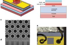
The on-chip laser sources are one of the key components in PICs, which are the optical analogies of the electric circuits but possess much higher transport speeds and much broader bandwidths. The hybrid integration of the on-chip laser sources, waveguides, optical processing components (e.g., splitters, filters, amplifiers, and modulators), and detectors can greatly increase the performances of the functional PICs, as shown in Fig. 1, where the different colors denote the different materials. The reason is that every nanophotonic device possesses its optimal materials and structures. The hybrid integration can combine the advantages of all kinds of materials and structures. For example, the CQDs are an ideal gain material, but they are not suitable for light guiding because of the large absorption at the lasing wavelengths[2]. Moreover, the sizes of CQD-based nanophotonic devices can’t break the diffraction limit. It is known that surface plasmon polaritons supported by the metallic nanostructures show subwavelength field confinements[3]. The hybrid integration of on-chip CQD lasers and subwavelength plasmonic waveguides can combine both the advantages of the high performances of the small CQD lasers (large gain, solution-processibility, low threshold, and high quality factor) and the plasmonic waveguides (deep subwavelength confinement). However, the precise hybrid integration is a challenge owing to the complexity of the hybrid structures and the damageability of the gain media in the multi-step micro/nanofabrications. To address the fabrication problem in the hybrid integration, Chen’s group developed the dark-field optical imaging technique with a position uncertainty of about 21 nm. By employing this simple and precise technique together with the high-resolution electron beam lithography, the small CQD lasers were accurately aligned with the silver nanowires without any damages[4]. As a result, the deep-subwavelength coherent sources (multimode, one-color single-mode, or two-color single-mode) with a mode area of only 0.008λ2 were output from the hybrid structures. This precise hybrid integration method would greatly facilitate the developments of the complex functional hybrid photonic–plasmonic circuits. For the hybrid integration of other materials (especially for new materials) and structures, the exploitation of more novel fabrication methods is eagerly desired.
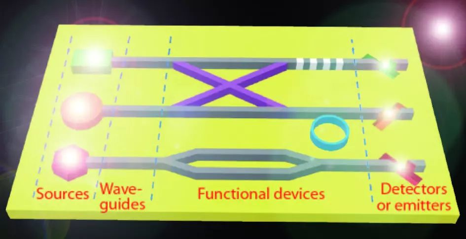
Figure 1. (Color online) Hybrid integration in photonic integrated circuits, which consist of the on-chip laser sources, waveguides, functional devices, and detectors (or emitters). The different colors denote the different materials.
AcknowledgementsThis work was supported by the National Basic Research Program of China (Nos. 2016YFA0203500, 2017YFF0206103), the National Natural Science Foundation of China (Nos. 91850103, 11674014, 61475005, 11525414, 11527901, 11134001), and the Beijing Natural Science Foundation (No. Z180015).
References
[1] Kagan C R, Lifshitz E, Sargent E H, et al. Building devices from colloidal quantum dots. Science, 2016, 353(6302), aac5523
[2] Rong L, Sun C, Shi K, et al. Room-temperature planar lasers based on water-dripping microplates of colloidal quantum dots. ACS Photonics, 2017, 4, 1776
[3] Chen J, Gan F, Wang Y, et al. Plasmonic sensing and modulation based on Fano resonances. Adv Opt Mater, 2018, 6, 1701152
[4] Rong K, Gan F, Shi K, et al. Configurable integration of on-chip quantum dot lasers and subwavelength plasmonic waveguides. Adv Mater, 2018, 30, 1706546
来源:bdtdsj 中科院半导体所
原文链接:http://mp.weixin.qq.com/s?__biz=MzI1OTExNzkzNw==&mid=2650448708&idx=2&sn=393addc553460ca3ceb3e317b62be4be&chksm=f273c55ac5044c4cbfd2b2134af63434bfe10d97ed0bb1d42d604d39f73aa0e0554810a45616&scene=27#wechat_redirect
版权声明:除非特别注明,本站所载内容来源于互联网、微信公众号等公开渠道,不代表本站观点,仅供参考、交流、公益传播之目的。转载的稿件版权归原作者或机构所有,如有侵权,请联系删除。
电话:(010)86409582
邮箱:kejie@scimall.org.cn
融入量子点设计的新型双面板太阳能窗户问世
半导体所等在高功率、低噪声量子点DFB单模激光器研究中获进展
染料激光器
量子级联激光器
高速超导磁悬浮列车、涌现拓扑现象、量子点激光器、量子计算及其应用、异构材料 | 本周直播物理讲座
基于平带的量子点光子晶体表面发射激光器,实现高功
GaN基蓝光与绿光激光器
量子物理学:通过量子隐形传输把点连起来

新型液晶激光器研究获进展

量子激光器:化“损失”为“收益”


科技工作者之家APP是专注科技人才,知识分享与人才交流的服务平台。
 微信
微信
 京公网安备11010202008424号